Indian semiconductor ecosystem: News, Updates & Discussions.

Buy something imported from not-China, solve yourself a headache.
I have a Siglent 1202 in my garage, I think I will buy him something similar siglent/rigol or may be a used keysight . He just wants something to verify accel calibration coefs.
 
I have a Siglent 1202 in my garage, I think I will buy him something similar siglent/rigol or may be a used keysight . He just wants something to verify accel calibration coefs.

I think even Siglent is just repackaged Chini maal. Rigol is original Chini maal, as is Hantek.
 
I think even Siglent is just repackaged Chini maal. Rigol is original Chini maal, as is Hantek.
Not repackaged, Siglent and Rigol are made in china brands, gW inst is made in taiwan. Even some of tek is now made in china, Keysight is made here, but price is ridiculously high.
 
  • Like
Reactions: randomradio
Not repackaged, Siglent and Rigol are made in china brands, gW inst is made in taiwan. Even some of tek is now made in china, Keysight is made here, but price is ridiculously high.

It's their own IP then. So yeah, go for anything that's non-Chinese IP, it will actually work.
 

India will consume semiconductors of $80 billion to manufacture electronics worth $300 billion: MoS IT​

The Minister of State for Electronics and IT Rajeev Chandrasekhar on Monday said India will consume semiconductors of about $70-80 billion to manufacture electronics products worth $300 billion by 2026 in line with the government's vision.


Chandrasekhar says the government will achieve the target of establishing a semiconductor ecosystem in India depending upon the interest it is getting from around the globe.

He was speaking on the eve of announcing the first conference on setting up the semiconductor ecosystem in the country -- Semicon India 2022 - that is expected to attract Semiconductor leaders from across the world.

He said, "Demand for digital devices and electronics products is only going up. If you have seen our electronics vision document, we have announced a target of $300 billion in electronic manufacturing, with $120 billion in exports. Our consumption, based on $300 billion electronics (production target by 2026), will be almost $70-80 billion of semiconductors," reported by PTI.

Semicon India programme entailed incentives to the tune of ₹76,000 crore.

As per the report, companies like Vedanta Foxconn JV, IGSS Ventures, and ISMC have submitted proposals to set up electronic chip manufacturing plants with a $13.6 billion investment. They have sought the support of $5.6 billion from the government under the ₹76,000 crore programme.

Further, Vedanta and Elest have proposed a projected investment of $6.7 billion to set up display manufacturing units -- used in mobile phones, laptops, etc. They have sought the support of $2.7 billion from the government under the scheme for setting up display fabs in India.

The minister stated that the applications are being processed at the moment and declined to provide an estimated timeline for their approval.

Prime Minister Narendra Modi will inaugurate the first-ever Semicon India 2022 Conference at 11 am, on 29th April 2022 in Bengaluru.

Chandrasekhar stated that Semicon India – 2022, a 3-day conference, is being organized to take forward the vision of PM Modi which is to make India a leader in electronics manufacturing, semiconductor design, manufacturing & innovation.

Chandrasekhar said that PM’s vision is to make India a significant player in the Global Semiconductor value chain. First time in the last 75 years- rapid decisive strides have been made in this space, he added. Semicon India 2022 conference will attract the best minds from across the world from the semiconductor industry, research & academia and will act as a big step in fulfilling PM’s vision of making India a global hub for electronics manufacturing and the semiconductor industry.

The ministry will organize Semicon India 2022 conference from April 29 – 01 May 2022 at ITC Gardenia, Bengaluru.

This conference will serve as the first roadshow in the series of a roadshow that the Ministry of Electronics & Information Technology will be organizing. Global experts from industry and academia involved in semiconductor design and manufacturing and key representatives from Government are proposed to participate in the event.

As per the ministry, India Semiconductor Mission (ISM) has been set up as an Independent Business Division within Digital India Corporation having administrative and financial autonomy to formulate and drive India’s long-term strategies for developing semiconductors and display manufacturing facilities and semiconductor design ecosystem. Envisioned to be led by global experts in the Semiconductor and Display industry, ISM will serve as the nodal agency for efficient, coherent, and smooth implementation of the schemes.
 
  • Like
Reactions: _Anonymous_
ISMC Announces Setting Up Of India's First Semiconductor Fab In Karnataka At An Investment Of $3 Billion


Coimbatore Emerges As Candidate For A Semiconductor Plant: Tata Group And Tamil Nadu Government In Talks Over Potential Investment


So finally the ball starts Rolling for semiconductor industry.... 😊
 
  • Love
Reactions: jetray
1)Make in India
2)Atma nirbhar
3)SP model
Only god knows what will happen to semi conductor industry three years from now.
 

India's First Semiconductor Chip Manufacturing Plant In Mysuru. How Much Water Will It Actually Need? An Estimate​

India's First Semiconductor Chip Manufacturing Plant In Mysuru. How Much Water Will It Actually Need? An Estimate

India's First Semiconductor Chip Manufacturing Plant In Mysuru. How Much Water Will It Actually Need? An Estimate​

International semiconductor consortium ISMC, led by Next Orbit Ventures and Israel's Tower Semiconductor as JV partner, signed a Rs 22,900-crore ($3 billion) agreement with the Karnataka government to set up a chip-manufacturing plant on 150 acres of land in Mysuru's Kochanahalli Industrial Area.

The Karnataka government is setting up an Electronics Manufacturing Cluster at Kochanahalli, located around 5 km from Mysuru Airport. The semiconductor plant is expected to generate 1,500 high-tech and high-quality jobs and at least10,000 ancillary jobs. The proposed plant is expected to provide a significant boost to the industrialisation of the district.

According to Ajay Jalan, ISMC Director and Next Orbit Founder and Managing Partner, the consortium selected Karnataka as the location for its fab factory due to water availability, the stable power situation in the state, access to talent, quality of life for talented engineers, incentive package offered by the state. He also praised the decisive and proactive approach of chief minister Basavaraj Bommai and his team.

ISMC was considering Dholera Investment Region in Gujarat as a possible site for the chip manufacturing plant. Suggestions have emerged that the state may have lost out due to water. However, the real reason is that Gujarat also does not have formidable electronic manufacturing and design ecosystem like Karnataka.

So how much water does semiconductor manufacturing need?
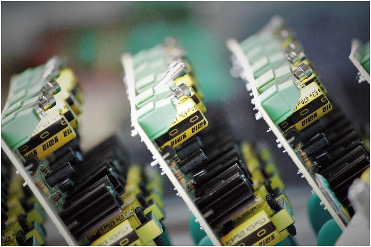
Semiconductor manufacturing is a water-intensive operation. Over a series of steps, semiconductors are built in layers on silicon wafers into integrated circuits (also called microchips). After each one of several dozen layers of semiconductors are added to the silicon wafer, it must be rinsed, requiring massive amounts of water. A great deal of this water is Ultra Pure Water (UPW), water that is thousands of times purer than drinking water.

A report in The Times Of India quoted Karnataka Rajya Raitha Sangha state president Badagalapura Nagendra as saying that industries in Mysuru district will harm the environment and that semiconductor manufacturing units require a lot of water. He also expressed fear that water would be diverted from agriculture to industry. However, business and industry groups have dismissed such claims pointing out that 40% of the water used is recycled.

Chip behemoth Intel reduced its water consumption by over 40 percent from previous levels in response to the arid conditions at the sites where its plants are located. Taiwan Semiconductor Manufacturing Co (TSMC) has embarked on several water conservation efforts. Advances in treatment of wastewater at semiconductor plants has led to recycling anywhere from 40 percent to 70 percent of water used in their processes

Here is an estimate of the water that would be required for the fab that ISMC is proposing to set up in Karnataka
1) International Semiconductors Consortium (ISMC) has proposed a fab that can handle 40,000 Wafer Starts Per Month (WSPM) of 300mm (i.e. 12 inches) size wafers at 65nm process nodes when running at full capacity.

Building the facility may take two years after approval, equipment and robotics setup will take one year, and tuning the process to run in a new production line after it is "copy-pasted" (production-grade technology transfer) by Tower Semiconductor may take six months to a year. This is assuming the project progresses smoothly and starts the clock after groundbreaking.

In the 5th year after groundbreaking, one can expect sellable chips to come out, but most likely at only about 30-40 per cent of the total capacity. By the end of 7 years, the capacity readiness and utilisation will hopefully go up closer to the unit's full capacity.
Here is an estimate of the water that would be required for the fab that ISMC is proposing to set up in Karnataka

2) This paper has a detailed study of water usage in various fabs in Taiwan. Let us take this table.

Water consumption efficiency of major TFT-LCD companies in Taiwan (data in 2015).


For Taiwan Semiconductor Manufacturing Company (TSMC), it says about 45 litres per wafer layer of an 8 inch (i.e. 200mm) wafer. The area of a 300mm wafer is 2.25 times, so the water needed will be about 45 X 2.25 or roughly 100 litres per wafer level. The Winbond number is for the 12-inch wafer itself and is 123 litre - a little more than what we calculated for TSMC. Let us assume that the ISMC fab may not be as efficient in water reuse and so, as a worst-case, uses 200 litres per wafer level.

3) For Now, what is a "level"? That is the number of "layers" of processing in a chip. For example, the creation of an active area is one level, the gate of the transistors is another layer, source and drain doping could be one or a few layers, contact to the active area is one level, and each of the further metal layers and the vias connecting them are such levels.

For those familiar with fabs, each level will need a separate photomask (reticle). The number of levels needed in the processing of chips will vary from chip to chip based on the process node and also the complexity of the chip itself.

If you take the chart here, 65nm process node Application Specific Integrated Circuit (ASIC) chips need about 35 mask levels. ISMC may not be making the same kind of chips as TSMC, but mask levels needed in 65nm is roughly the same (give or take a few).


TSMC masc count.
TSMC masc count.


To summarise - a maximum of 200 litres of water per wafer layer, 35 such layers, means roughly 7000 litres of water to process one wafer. (As a side note, one wafer will have 100s of chips based on the size of each chip, but that number does not change the water calculation as we are calculating for the whole wafer).

According to another estimate, 2200 gallons (8327 litres) of water is needed per 30cm (i.e. 300mm or 12 inch) wafer. While this 2013 estimate does not explicitly mention which process node they used for calculation, it is likely to be for 40nm which needs slightly more as the number of masks increases. So for 65nm, we can safely assume 8000 litres.

Note that these calculations already consider that to get 1000 litres of Ultrapure water, you need to start with about 50% more "municipal water".
5) Now, to get the per day usage, we multiply by the capacity. 40000 WSPM (if running at full capacity) is about 1400 wafers per day. 1400 X 8000 litres = 11,200,000 .. or in other words, about 11 Million Litres Per Day(MLD). On the practical side, it is likely to be more like 7 or 8 MLDs because we have assumed the maximum in every step.

As a way of comparison, Vedanta has reportedly requested 40 MLDs of water for the fabs they are proposing to set up (their proposed fab is 28nm process node and, in full capacity, is hoping to run 80,000 or even 1,00,000 WSPM and hence higher water requirement.

Calculating Fab Water Requirement
Is 10 MLD a lot of water?

a) The per person availability of water in India is predicted to be 1.465 MLD by 2025. So 10 MLD equals "available" water for about seven people every day. In an entire year, about 2500 people (note: Availability is not the same as usage; average water used by Indians for drinking and domestic needs is 135 litres based on this detailed study).

b) How about water usage in other sectors?
A study by Observer Research Foundation points out that most of India's usable water goes into agriculture, and even by 2025, it will still be around 83.3 per cent. India's textile industry, as per this article, uses 1608 MLD.

c) This article mentions that India's 300 cities generate about 40,000 MLDs of domestic wastewater that is untreated and is discharged into rivers.

d) 1 cusec is approximately 28 litres per second. So, for example, when 10,000 cusecs of water are released, that is 2,80,000 litres per second. In about 35 seconds, you get 10 million litres.
(With key inputs from Arun Mampazhy)
 
Groundbreaking ceremony for Indian Semiconductor unit in 2-3 months:

India's decades-old dream to become a semiconductor manufacturing hub is finally moving in the right direction. The Semiconductor scheme announced in December 2021 has received excellent progress, said the minister. "Typical decision on semiconductor happens in a timeframe of 14 to 18 months, all over the world. On January 1 of this year is when we uploaded the applications. Today we are in a position where in the coming two or three months, we should be having the first groundbreaking ceremony for Indian semiconductor manufacturing units." Plus, the minister promised that India would have multiple fabs. But India needs to accept that the world is far ahead of us. So, India will have to really accelerate this journey. It will take India definitely 5-6 years to become a major player in semiconductor manufacturing.

India will become chip design capital for the world:

While the minister said it be challenging to answer the question by when the country become the chip manufacturing capital of the world, he said India will become the chip design capital of the world. "Today we have close to 55,000 design semiconductor engineers working for various companies. And as part of our semiconductor program, we have brought out a design-led scheme where the engineers who want to try out their luck in designing semiconductor chips, they can come out they can use common facilities which are getting developed at C-DAC unit in Pune and startup their venture. If they succeed or do not succeed, there is a great ecosystem already there. So I can confidently say that within the next five to six years, we will become a great semiconductor design capital of the world. We will use that capability to feed into our semiconductor manufacturing also."
 

India has joined the global chip race. Question is, should it fly solo?​

India’s bid to join the global chip-manufacturing rush is likely to be its biggest “industrial policy” gambit in a long time. Such government-directed policy intervention went out of fashion decades ago as the free trade mantra caught on.

It has now made a comeback as the supply disruption of Covid-Ukraine has made every major economy conscious of strategic vulnerabilities. The nightmare scenario would be if Taiwan, which accounts for more than half the global chip supply, is attacked by China, which accounts for half the global demand.

Chips, or integrated circuits imprinted on silicon wafers, are at the heart of every kind of manufacturing industry from automobiles to telecom gear, and from defence equipment to solar panels. They will become even more so in a world of artificial intelligence and electric cars, which need many more chips than petrol-driven ones.

Yet, the massive dollops of cash needed for cutting-edge research and super-expensive production facilities have concentrated the chip-making business in half a dozen companies that command global dominance.

Now, government after government is throwing billions of dollars at chip manufacture, hoping to improve market share. The US has offered incentives totalling USD 52 billion. The European Union is topping up an earlier offer of USD 30 billion. China reportedly subsidises its chip manufacture to the extent of USD 15 billion annually. Samsung plans to invest USD 200 billion in new chip factories.

Can India, headed to become the third-largest economy in a decade and one of the world’s largest markets for a range of chip-based products, be left sitting on its hands? It has already offered an unprecedented USD 10 billion as capital subsidy. Is that enough? And is self-reliance the right approach in a mega-buck game, or better to be part of a network?

Chip manufacture needs a complex ecosystem. You need the tools that will populate factories (an area of Japanese leadership), the photolithography equipment that photo-prints circuits on silicon wafers (a Dutch speciality), and the materials that go into the finished product — for instance, neon gas and palladium, for which Russia and Ukraine have been leading suppliers.

China moved early to procure some rare earths and minerals, to counter the US which has corralled 10 other countries into a Minerals Security Partnership. India has been excluded.

Result: Inter-dependence is unavoidable. The US leads in logic chip design, South Korea in memory chips. Intel and others outsource wafer fabrication to Taiwan. Japan’s chip industry is still focused on older technology (there is a market for this). Intel in the US has not yet broken through the 10 nm (one-hundred thousandth of a millimetre) barrier, whereas the Taiwan Semiconductor Manufacturing Company and Samsung produce 3 nm chips. China has just broken through to 7 nm, while Japan and the US are jointly working on 2 nm technology. More such alliances may evolve.

What is India trying to do? Its chip-making gambit is part of a broader, incentive-based thrust into electronics manufacturing. It has been buoyed by the initial success in mobile handset manufacture. Whether it will succeed in making display units (for laptops, handsets, etc), another focus area, remains to be seen.

Chip manufacturers proposing to locate in India might look at mid-range chips (28 nm) used by the automobile industry and some smart phones.

Inevitably, there is debate on the full-spectrum approach vs specialisation. The country has strengths in chip design, and a natural advantage in the labour-intensive part of chip-making (assembly, testing and packaging). It could also do well in downstream product assembly, as with mobile handsets. Some component or sub-assembly makers might invest here to feed assembly lines. In time, an ecosystem could develop with global linkages.

The full-spectrum approach, which the government prefers, seeks to replace imports of both chips and downstream products, though upstream import dependencies for materials and production equipment would remain. And since the wafer-fabrication process is capital-intensive, with a demanding production process in the midst of constant technology change, you may need to keep committing billions.

Still, the government apparently feels India cannot afford to stay out of this game. We will know in a few years whether this is “vaulting ambition which o’erleaps itself” or breakthrough strategy.