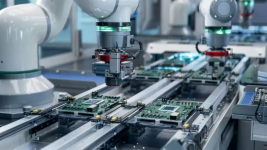
Indian semiconductor ecosystem: News, Updates & Discussions.

 
It is not either legacy nodes or advanced nodes. We need all the semicon plants we can get.
But there is implicit ban on advanced nodes plant in India (<14nm), which we should be having one way or another to be truly self reliant.
See the reason given by TSMC to India, Qatar etc, when asked to setup advanced node:


See the semicon industry is very large with very niche players from Japan, Germany etc whom whole industry depends for these advanced nodes and TSMC is just a integrator of all these inputs(not discounting them for running a fab, they did good). Even the ASML of Dutch depends on very specific inputs from US and Germany, that is why when US banned ASML from exporting their EUV to China ASML stayed silent because they themselves depend on US tech.


Ideally, apart from this push to get fabs we should focus on one particular area of semicon either the design softwares or photoresists or lenses etc. So that we too can integrate in the supply chains globally and become indispensable like how Japan, Germany etc are.
The latest EUV machine ASML makes was built a lot on US Gov and Intel sponsored research in Argonne National Labratory and other US gov sites even including Lawrence Livermore iirc. America is very advanced in laser technology, they tried making lasers to shoot down nuclear missiles and they even tried to make hydrogen bombs using lasers to de compress the secondary fusion stage instead of relying on a primary plutonium stage (they failed after spending billions but they gaines tons of experience). So its safe to say without US approval ASML EUV machines can't move an inch.

China is trying very hard to make their own EUV machines but idt it will happen in the next 5-10 years unless they do cyber espionage on US or ASML companies. To reach EUV tech American labs did research on lasers from 1970s! So China will remain stuck at 5 nm for the foreseeable future which is still a formidable capability. Wtr to India, first we need to focus on legacy nodes and defeating Chinese over capacity in legacy nodes. Imo it's wrong to jump to advanced nodes before we build a huge production capacity for legacy nodes. All of our critical systems and defence tech use legacy nodes of up to 28 nm. We need to gain self sufficiency here first. Second of all we need to form indigenous design companies who can make SoCs and chips on this process bcuz many of our engineers are designing chips for IBM, Google etc.
 
  • Like
Reactions: Asterion Moloc
It is not either legacy nodes or advanced nodes. We need all the semicon plants we can get.
But there is implicit ban on advanced nodes plant in India (<14nm), which we should be having one way or another to be truly self reliant.
See the reason given by TSMC to India, Qatar etc, when asked to setup advanced node:


See the semicon industry is very large with very niche players from Japan, Germany etc whom whole industry depends for these advanced nodes and TSMC is just a integrator of all these inputs(not discounting them for running a fab, they did good). Even the ASML of Dutch depends on very specific inputs from US and Germany, that is why when US banned ASML from exporting their EUV to China ASML stayed silent because they themselves depend on US tech.


Ideally, apart from this push to get fabs we should focus on one particular area of semicon either the design softwares or photoresists or lenses etc. So that we too can integrate in the supply chains globally and become indispensable like how Japan, Germany etc are.
Wtr to your last point, I 1000000% agree. We need to become masters of critical tech which world depends on. It needs a national push. Germany has huge experience in lenses, so idt we can compete with them in that area yet. We have a strong chance for design software. Even China still depends on US for EDA software. We need to go all in in this area as software is one of our strong suits. Iirc we even made a software for LCA Tejas which even Airbus licensed from us. Unrelated to semiconductors but shows our potential in software.
 
The latest EUV machine ASML makes was built a lot on US Gov and Intel sponsored research in Argonne National Labratory and other US gov sites even including Lawrence Livermore iirc. America is very advanced in laser technology, they tried making lasers to shoot down nuclear missiles and they even tried to make hydrogen bombs using lasers to de compress the secondary fusion stage instead of relying on a primary plutonium stage (they failed after spending billions but they gaines tons of experience). So its safe to say without US approval ASML EUV machines can't move an inch.

China is trying very hard to make their own EUV machines but idt it will happen in the next 5-10 years unless they do cyber espionage on US or ASML companies. To reach EUV tech American labs did research on lasers from 1970s! So China will remain stuck at 5 nm for the foreseeable future which is still a formidable capability. Wtr to India, first we need to focus on legacy nodes and defeating Chinese over capacity in legacy nodes. Imo it's wrong to jump to advanced nodes before we build a huge production capacity for legacy nodes. All of our critical systems and defence tech use legacy nodes of up to 28 nm. We need to gain self sufficiency here first. Second of all we need to form indigenous design companies who can make SoCs and chips on this process bcuz many of our engineers are designing chips for IBM, Google etc.
Yes, as I quoted my old post US formed a LLC called EUV-LLC with intel and others later ASML was also roped in and tech transfer happened. Cymer a US based company makes these laser source for EUVL machines, ASML bought it in 2013. (pg 13 in pdf)

You can see S&T review articles from LLNL about their and US contribution to EUVL tech

Coming to China, I don't follow them much. But you are right there is so much to catch-up for Chinese if they approach the same path. I think they have DUV lense based setup already and with it you can try 7nm nodes(I may be wrong) but yield will be less. The tricky thing with sanctions is, even with lower yield these 7nm or whatever advanced china can make will be the only game in town. So, chinese domestic customers will not care but exports will be hit, cause anyone will choose similar or even lower priced TSMC manufactured advanced chips than chinese ones.
GOI should learn from US strangulation of chinese and prepare for it covertly atleast to maintain current compute levels for consumers in India. For Strategic puproses as you said anyway they are in legacy nodes and yield is not required for them.

Wtr to your last point, I 1000000% agree. We need to become masters of critical tech which world depends on. It needs a national push. Germany has huge experience in lenses, so idt we can compete with them in that area yet. We have a strong chance for design software. Even China still depends on US for EDA software. We need to go all in in this area as software is one of our strong suits. Iirc we even made a software for LCA Tejas which even Airbus licensed from us. Unrelated to semiconductors but shows our potential in software.
Yep, just one critical area where you are the market leader is enough to get leverage. But maintaining that market leader position requires substantial efforts and R&D investment continuously. Even Photoresists and chemicals side can be tried. Aim for one area and put all resources there, we can have market leader in that segment, requires smart policy and execution.

Software(EDA) is also US strong suite, so care should be taken that US companies should not buy out our companies.
Recently Zoho dropped their Fab plan, I hope they try to venture into EDA space atleast.
 
GsfY1yUX0AA8BtC
 
Tata Electronics, BEL sign MoU to power India’s semiconductor and electronics push

Tata Electronics and Bharat Electronics have signed an MoU to collaborate on semiconductor and electronics solutions, advancing India’s self-reliance goals across chip design, fabrication, OSAT, and defence-grade electronics components.

By Sheersh Kapoor
June 6, 2025, 4:35:25 PM IST (Published)
1749232483823.png

Tata Electronics and Bharat Electronics Limited (BEL) on Wednesday signed a Memorandum of Understanding (MoU) to jointly explore semiconductor and advanced electronics solutions aligned with India’s push for self-reliance in the sector.

The MoU was formalised on 5 June at Bombay House, Tata Group’s Mumbai headquarters, by Dr Randhir Thakur, CEO and MD of Tata Electronics, and Manoj Jain, CMD of BEL. BEL, a Navratna defence PSU, specialises in design and manufacture of advanced electronics systems for strategic and civilian use.

The collaboration will focus on identifying and developing end-to-end solutions spanning semiconductor fabrication (Fab), Outsourced Semiconductor Assembly and Test (OSAT), and chip design services.

Potential components include microcontrollers (MCUs), systems-on-chip (SoCs), monolithic microwave integrated circuits (MMICs), and other processors for BEL’s current and future needs.

The two companies also plan to co-develop optimal manufacturing practices through knowledge sharing and joint capability development, supporting India's broader vision to reduce import dependency in critical electronics and semiconductor domains.

Ahead of the announcement, shares of BEL closed at ₹390.70, down 0.76% on the BSE.

Tata Electronics, BEL sign MoU to power India’s semiconductor and electronics push - CNBC TV18