IIT BOMBAY AND ISRO’S SCL INDIGENOUSLY AUGMENT THEIR 180-NANOMETER TECHNOLOGY FOR VERSATILE AND POWERFUL CHIPS
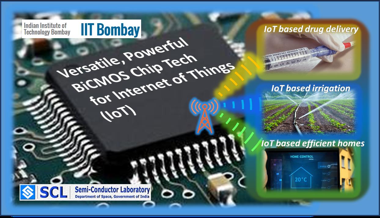
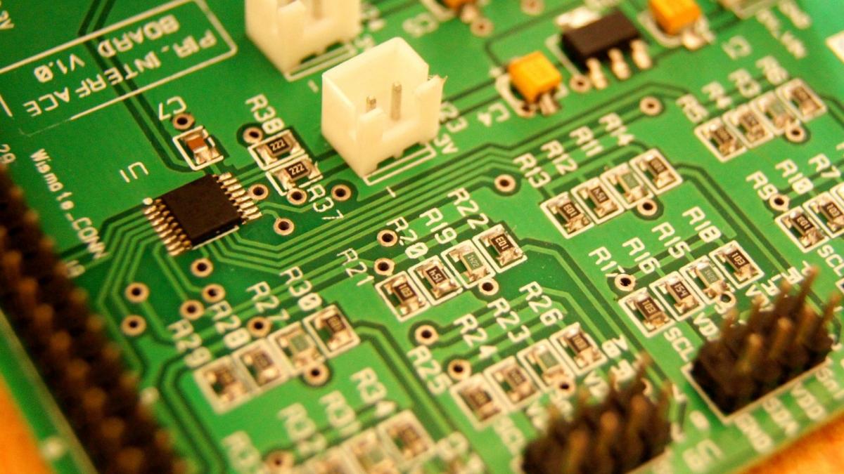
The transistor, a semiconductor device used to boost or switch electronic signals, is a widely used component in almost every electronic device, big and small. In fact, it is often considered as one of the greatest inventions of the 20th century. As electronic devices become sophisticated, and find new applications, different types of transistors are being designed and developed to suit those applications. Among them is the Bipolar Junction Transistor (BJT), a transistor that uses both electron and hole charge carriers (bipolar) for its operation. It is now touted to play a big role in the Internet of Things (IoT) applications.
But how does this transistor fit in the bigger landscape? Almost every IoT solution needs sensors, which collect data from their surroundings. This data (or signals) could either be digital like the images captured by a camera, or analog as in the case of audio signals. Processing the two types of signals needs a versatile technology platform that can work with mixed signals and result in optimal performance. While the Complementary Metal Oxide Semiconductor (CMOS) transistors handle digital signals, BJTs work with analog signals. Bi-CMOS (short for Bipolar-CMOS) technology combines the two transistor technologies in one chip.
In space and communication related applications, BJTs are used in antennas for communications. It is compatible with CMOS. It can drive long transmission lines to enable communication chips working with signals of very high frequency (250MHz -20GHz). ISRO’s primary interest is to develop such light-weight, energy-efficient, high-frequency chips needed for payloads in satellites and rockets. Conventional frequency amplifiers like gallium arsenide (GaAs) or gallium nitride (GaN) are stand-alone and result in bulkier chips when coupled with CMOS based signal-processing units.
Now, researchers at the Indian Institute of Technology - Bombay (IIT-B), in a collaborative effort with ISRO’s Semi-Conductor Labs (SCL), Chandigarh, have developed a completely indigenous Bipolar Junction Transistor (BJT) that can work with Bi-CMOS. This development was the result of a year long research led by Prof. Udayan Ganguly and Dr. Piyush Bhatt. Prof. Ganguly, an Associate Professor at the Department of Electrical Engineering, IIT-B also the co-Principal Investigator at the Centre of Excellence in Nanoelectronics (CEN) at IIT-B.
India has two semiconductor manufacturing organizations - STAR-C (a unit of SITAR by Govt. of India) and the SCL, which is the most advanced fabrication facility in the country, producing high frequency, low power digital CMOS for strategic and national needs. However, international tech giants have largely pioneered cutting-edge semiconductor technologies. These exclusive technologies may be availed through technology transfers -- the process of transferring scientific findings from one organization to another for the purpose of further development and commercialization.
“To have unfettered access to such technologies for national needs, indigenous technology development is a must” remarks Prof. Ganguly, citing the reasons for the need to augment this production technology indigenously. He also points out two important gaps that have stymied indigenous technology development -- the gap in CMOS technology development and manufacturing expertise, and the gap in advanced semiconductor manufacturing.
Enabling the growth of ESDM
In the wake of India’s growing Electronics System Design & Manufacturing (ESDM) sector, and estimates that the Indian electronics' market would grow to be $228 billion in 2020, there is also a need for innovations in circuit design and manufacturing to go beyond the reach of large design houses with connections to giant foundries. “Smaller design teams have access to only standard technologies available commercially”, opines Prof. Ganguly, citing how SCL’s ability to develop custom technologies will add a further edge to demonstrate proof of concept IoT technologies. “This could help develop innovative products for electronic sensing and control in various nationally relevant environments like medical, agriculture, efficient home, public places and factories”, he adds.
In addition, the Centre for Excellence in Nanoelectronics (CEN) -- a collaborative project between IIT-B and IISc, provides a world-class expertise that excels in semiconductor device design, fabrication, modeling and reliability. With the development of BJT, technology development with Indian organizations has reached new levels, surpassing the persistent challenge to interface with Indian manufacturing houses in electronics. “CEN has enabled the group to have excellent in-house ‘hands-on’ expertise in new technology development. In addition, the group has worked with various international research and manufacturing houses to develop key technologies”, says Prof. Ganguly. He further adds that “Every bit of knowledge, technique and idea in our research labs can translate into either commercial or strategic products of the future.”
The transistor, a semiconductor device used to boost or switch electronic signals, is a widely used component in almost every electronic device, big and small. In fact, it is often considered as one of the greatest inventions of the 20th century. As electronic devices become sophisticated, and find new applications, different types of transistors are being designed and developed to suit those applications. Among them is the Bipolar Junction Transistor (BJT), a transistor that uses both electron and hole charge carriers (bipolar) for its operation. It is now touted to play a big role in the Internet of Things (IoT) applications.
But how does this transistor fit in the bigger landscape? Almost every IoT solution needs sensors, which collect data from their surroundings. This data (or signals) could either be digital like the images captured by a camera, or analog as in the case of audio signals. Processing the two types of signals needs a versatile technology platform that can work with mixed signals and result in optimal performance. While the Complementary Metal Oxide Semiconductor (CMOS) transistors handle digital signals, BJTs work with analog signals. Bi-CMOS (short for Bipolar-CMOS) technology combines the two transistor technologies in one chip.
In space and communication related applications, BJTs are used in antennas for communications. It is compatible with CMOS. It can drive long transmission lines to enable communication chips working with signals of very high frequency (250MHz -20GHz). ISRO’s primary interest is to develop such light-weight, energy-efficient, high-frequency chips needed for payloads in satellites and rockets. Conventional frequency amplifiers like gallium arsenide (GaAs) or gallium nitride (GaN) are stand-alone and result in bulkier chips when coupled with CMOS based signal-processing units.
Now, researchers at the Indian Institute of Technology - Bombay (IIT-B), in a collaborative effort with ISRO’s Semi-Conductor Labs (SCL), Chandigarh, have developed a completely indigenous Bipolar Junction Transistor (BJT) that can work with Bi-CMOS. This development was the result of a year long research led by Prof. Udayan Ganguly and Dr. Piyush Bhatt. Prof. Ganguly, an Associate Professor at the Department of Electrical Engineering, IIT-B also the co-Principal Investigator at the Centre of Excellence in Nanoelectronics (CEN) at IIT-B.
“The technology adds High Frequency Circuits to the existing digital CMOS technology. It enables high frequency communications and analog/mixed chips for various applications like IoT and space”, says Prof. Ganguly. “Bi-CMOS technology with integrated BJT based amplifiers reduces form factor, power consumption and cost – all essential for space applications”, he adds.
Making in India - a strategic moveIndia has two semiconductor manufacturing organizations - STAR-C (a unit of SITAR by Govt. of India) and the SCL, which is the most advanced fabrication facility in the country, producing high frequency, low power digital CMOS for strategic and national needs. However, international tech giants have largely pioneered cutting-edge semiconductor technologies. These exclusive technologies may be availed through technology transfers -- the process of transferring scientific findings from one organization to another for the purpose of further development and commercialization.
“To have unfettered access to such technologies for national needs, indigenous technology development is a must” remarks Prof. Ganguly, citing the reasons for the need to augment this production technology indigenously. He also points out two important gaps that have stymied indigenous technology development -- the gap in CMOS technology development and manufacturing expertise, and the gap in advanced semiconductor manufacturing.
“While electronics is one of the top research intensive area globally, India has not had a significant stake until the Centres for Excellence in Nanoelectronics (CENs) were seeded at IIT-B and IISc-Bangalore by the Ministry of Electronics”, he says adding that today, these centres draw international talent and are led by professors with first-hand technology development experience. Pointing out the need for fabrication facilities, he adds -- “While the electronics policy of 2017 claims that electronics imports will outstrip oil imports by 2020, the mega-fab creation in India is still under work.”
In this context, the development of the indigenous BJT is indeed a milestone for the CEN at IIT-B. The technology can, not only severe strategic applications in the areas of space and defense, but also in the development of digital and analog chips. Going forward, these chips can be developed and manufactured by SCL, or can be expanded for other corporate players to enter the business, leveraging SCL capabilities as a pilot line for scale-up.
Enabling the growth of ESDM
In the wake of India’s growing Electronics System Design & Manufacturing (ESDM) sector, and estimates that the Indian electronics' market would grow to be $228 billion in 2020, there is also a need for innovations in circuit design and manufacturing to go beyond the reach of large design houses with connections to giant foundries. “Smaller design teams have access to only standard technologies available commercially”, opines Prof. Ganguly, citing how SCL’s ability to develop custom technologies will add a further edge to demonstrate proof of concept IoT technologies. “This could help develop innovative products for electronic sensing and control in various nationally relevant environments like medical, agriculture, efficient home, public places and factories”, he adds.
In addition, the Centre for Excellence in Nanoelectronics (CEN) -- a collaborative project between IIT-B and IISc, provides a world-class expertise that excels in semiconductor device design, fabrication, modeling and reliability. With the development of BJT, technology development with Indian organizations has reached new levels, surpassing the persistent challenge to interface with Indian manufacturing houses in electronics. “CEN has enabled the group to have excellent in-house ‘hands-on’ expertise in new technology development. In addition, the group has worked with various international research and manufacturing houses to develop key technologies”, says Prof. Ganguly. He further adds that “Every bit of knowledge, technique and idea in our research labs can translate into either commercial or strategic products of the future.”
And what does a success story like this mean for the country’s educational institutes that are aiming to be the best in the world? “Success stories like this percolate through the entire community nationally to serve as examples to emulate”, signs off Prof. Ganguly.


 .
.